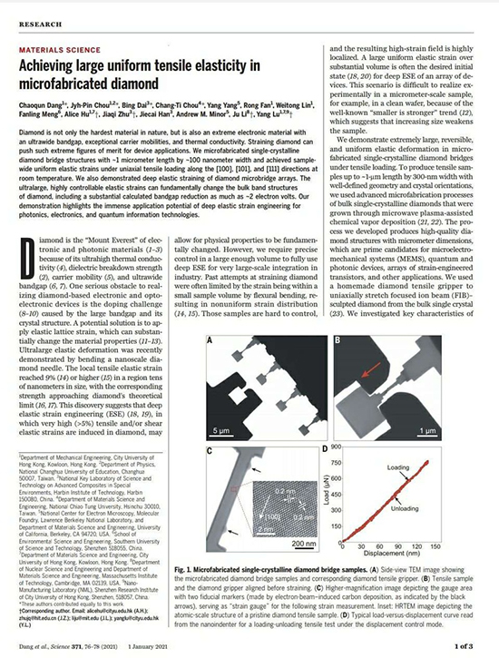
Harbin University of Technology News (Aerospace/Text) On January 1, 2021, our university, in cooperation with the City University of Hong Kong, the Massachusetts Institute of Technology and other units, demonstrated the uniform deep elastic strain of microcrystalline diamond arrays for the first time through nanomechanical methods.
This study highlights the great application potential of deep elastic strain engineering in photonics, electronics and quantum information technology. The research results are entitled "Achieving large uniform tensile elasticity in microfabricated diamond", published in the Science online. Professor Zhu Jiaqi from the Academician Han Jiecai's team and the young teacher Dai Bing are the co-authors (Lu Yang, Li Ju, Zhu Jiaqi, Alice Hu) and the co-first authors (Dang Chaoqun, Jyh-Pin Chou, Dai Bing, Chang-Ti Chou) respectively. Our school is a co-corresponding author and co-first author unit.
Diamond has high hardness, ultra-wideband gap, excellent carrier mobility and excellent thermal conductivity. It is one of the basic materials for realizing electrons, photoelectrons and quantum chips in the "post-Moore" era. At present, the biggest technical obstacle is to achieve effective regulation of band gap. Due to the compact structure of diamond, conventional N-type doping currently is in a slow progress. This study finds that through super-large elastic strain regulation, the energy band structure of diamond can be fundamentally changed, thus providing basic and subversive solutions for elastic strain engineering and the application of single crystal diamond devices.
Nano-scale diamond needles have been proved to have super-large elastic deformation, with local tensile elastic strains of more than 9%, indicating that deep elastic strain engineering (ESE) produces very high (> 5%) tensile and shear elastic strains in diamonds. However, the above-mentioned strain attempts are often limited to bending in the volume of small samples, resulting in uneven strain distribution and generating highly localized high strain field. It will be more academic and engineering significance to achieve large uniform elastic strain in wafer-level and micron-scale samples to make full use of deep elastic strain engineering for large-scale integrated processing of diamond devices.
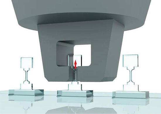
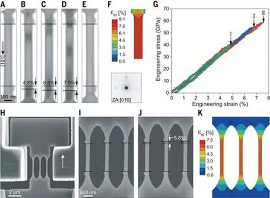
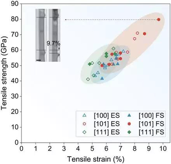
In this study, the structure of single crystal diamond bridges with a length of about 1 micron and a width of about 100 nanometers were finely processed along [100], [101] and [111] at room temperature. Uniform elastic strains in the sample range were obtained under single-axis tensile loads. By calculation, up to 2eV of the band gap reduction of the single crystal diamond can be achieved.
Academician Han Jiecai and Professor Zhu Jiaqi's team have been engaged in the research and development of large-scale single crystal diamonds, cutting-edge devices and equipment for a long time. With the support of the National Key R&D Program, the National Natural Science Foundation Program and other projects, they have achieved initial results in in-inch single crystal diamonds, diamond enhanced thermal conductivity devices, sun blind ultraviolet detection, nuclide batteries and other aspects, which can effectively support the improvement of our school's basic research and major engineering research and development capabilities.


Research results published


Loading and unloading tensile experiment along the [101] direction

[100], [101] and [111] oriented diamond statistical tensile results


