HIT All Media. Recently, the Institute of Special Ceramics, School of Materials Science and Engineering, Harbin Institute of Technology (HIT), has made important progress in the field of ultra-low power bionic photosynaptic devices and chips. The relevant results were published in Advanced Materials (IF 30.849), an influential journal in the field of Materials, with the paper entitled “Indium-induced Surface Charge Doped with Molybdenum Disulfide Ultra-low Power Photosynapse for Bionic Eyes”. HIT is the only communication unit for this paper. Doctoral student Hu Yunxia is the first author of this paper and Professor Hu Ping’an is the corresponding author of this paper.
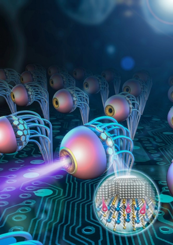
The research was inspired by the biological eye. The bionic eye has excellent imaging functions such as wide field of vision and low aberration, which can be applied to artificial intelligence equipment such as robots. The current vision system is usually composed of photodetectors, memory and processing units. It is a Von Neumann architecture mode with the separation of sensing, storage and computing, which has the problem of power consumption wall and storage wall, resulting in high energy consumption and difficulty in performing complex image learning and processing tasks. Therefore, it is of great significance to develop a vision system with a non-Von Neumann framework integrating sensing and storage of multifunctional optoelectronic devices. Among them, neuromorphic photosynaptic devices can respond to light stimuli and have good synaptic plasticity, which can combine the visual system and brain functions together. However, at present, neuromorphic photosynaptic devices have problems such as high power consumption and difficulty in realizing surface processing integration.
In order to solve these problems, Hu Ping’an’s research group added a discontinuous electron injection layer (indium layer) on the surface of the device channel two-dimensional semiconductor (MoS2), which effectively reduced the power consumption of the photosynaptic device to as low as 68.9 argyles per pulse, far less than the current international reported value of similar devices (> 1 picojoule). In addition, this study overcomes the problem of material growth and device processing integration on curved surfaces, and constructs a hemispherical electronic retina composed of Neurosynaptic device arrays, which realizes image sensing and learning functions. This work provides a new strategy for the performance regulation of neuromorphic photosynaptic devices and vision chips.
Hu Ping’an’ research group is engaged in the research of large-size two-dimensional single crystal wafer growth (graphene, hexagonal boron nitride, etc.) and photoelectric devices, has obtained high-performance van der Waals metal-insulator-semiconductor photoelectric detectors through valence band matching optimization, and developed low optical writing energy multi-bit optoelectronic memory based on selenium disulfide/hexagonal boron nitride/graphene heterostructure. These results were published online in the journals of Advanced Functional Materials (https://doi.org/10.1002/adfm.202104359) and Small (https://doi.org/10.1002/smll.202104459), and were invited to publish a review article entitled "Vertical transistors with sub1nm Channels" in Nature Electronics (201, 4,325-325).
The above research is strongly supported by the Key Laboratory of Microsystems and Microstructure Manufacturing of the Ministry of Education and the State Key Laboratory of Robotics and Systems.
The original link: https://doi.org/10.1002/adma.202104960


